|
Part Number |
Description |
|
QP4H-DP1M30WG |
100G QSFP28 DAC passive cable 30AWG 1m |
|
QP4H-DP2M30WG |
100G QSFP28 DAC passive cable 30AWG 2m |
|
QP4H-DP2.5M28WG |
100G QSFP28 DAC passive cable 28AWG 2.5m |
|
Parameter |
Symbol |
Min |
Typical |
Max |
Unit |
Note |
|
Differential Impedance |
TDR |
90 |
100 |
110 |
Ώ |
|
|
Insertion loss |
SDD21 |
-16.06 |
-8 |
dB |
At 13.28 GHz |
|
|
Differential Return Loss |
SDD11 SDD22 |
-12.45 |
See 1 |
dB |
At 0.05 to 4.1 GHz |
|
|
-3.12 |
See 2 |
dB |
At 4.1 to 19 GHz |
|||
|
Common-mode to common-mode output return loss |
SCC11 SCC22 |
-2 |
dB |
At 0.2 to 19 GHz |
||
|
Differential to common-mode return loss |
SCD11 SCD22 |
-12 |
See 3 |
dB |
At 0.01 to 12.89 GHz |
|
|
-10.58 |
See 4 |
At 12.89 to 19 GHz |
||||
|
Differential to common Mode Conversion Loss |
SCD21-IL |
-10 |
dB |
At 0.01 to 12.89 GHz |
||
| See 5 |
At 12.89 to 15.7 GHz |
|||||
|
-6.3 |
At 15.7 to 19 GHz |
|||||
|
Channel Operating Margin |
COM |
-3 |
dB |
|||
Notes:
|
||||||
|
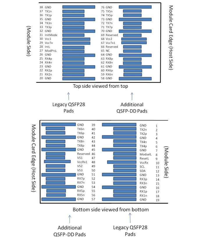
Pin |
Logic |
Symbol |
Description |
|
1 |
GND |
Ground |
|
|
2 |
CML-I |
Tx2n |
Transmitter Inverted Data Input |
|
3 |
CML-I |
Tx2p |
Transmitter Non-Inverted Data Input |
|
4 |
GND |
Ground |
|
|
5 |
CML-I |
Tx4n |
Transmitter Inverted Data Input |
|
6 |
CML-I |
Tx4p |
Transmitter Non-Inverted Data Input |
|
7 |
GND |
Ground |
|
|
8 |
LVTTL-I |
ModSelL |
Module Select |
|
9 |
LVTTL-I |
ResetL |
Module Reset |
|
10 |
Vcc Rx |
+3.3V Power Supply Receiver |
|
|
11 |
LVCMOS- |
SCL |
2-wire serial interface clock |
|
I/O |
|||
|
12 |
LVCMOS- |
SDA |
2-wire serial interface data |
|
I/O |
|||
|
13 |
GND |
Ground |
|
|
14 |
CML-O |
Rx3p |
Receiver Non-Inverted Data Output |
|
15 |
CML-O |
Rx3n |
Receiver Inverted Data Output |
|
16 |
GND |
Ground |
|
|
17 |
CML-O |
Rx1p |
Receiver Non-Inverted Data Output |
|
18 |
CML-O |
Rx1n |
Receiver Inverted Data Output |
|
19 |
GND |
Ground | |
|
20 |
GND |
Ground | |
|
21 |
CML-O |
Rx2n |
Receiver Inverted Data Output |
|
22 |
CML-O |
Rx2p |
Receiver Non-Inverted Data Output |
|
23 |
GND |
Ground | |
|
24 |
CML-O |
Rx4n |
Receiver Inverted Data Output |
|
25 |
CML-O |
Rx4p |
Receiver Non-Inverted Data Output |
|
26 |
GND |
Ground | |
|
27 |
LVTTL-O |
ModPrsL |
Module Present |
|
28 |
LVTTL-O |
IntL |
Interrupt |
|
29 |
Vcc Tx |
+3.3V Power supply transmitter | |
|
30 |
Vcc1 |
+3.3V Power supply | |
|
31 |
LVTTL-I |
LPMode |
Low Power Mode |
|
32 |
GND |
Ground | |
|
33 |
CML-I |
Tx3p |
Transmitter Non-Inverted Data Input |
|
34 |
CML-I |
Tx3n |
Transmitter Inverted Data Input |
|
35 |
GND |
Ground | |
|
36 |
CML-I |
Tx1p |
Transmitter Non-Inverted Data Input |
|
37 |
CML-I |
Tx1n |
Transmitter Inverted Data Input |
|
38 |
GND |
Ground | |
|
39 |
GND |
Ground | |
|
40 |
CML-I |
Tx6n |
Transmitter Inverted Data Input |
|
41 |
CML-I |
Tx6p |
Transmitter Non-Inverted Data Input |
|
42 |
GND |
Ground | |
|
43 |
CML-I |
Tx8n |
Transmitter Inverted Data Input |
|
44 |
CML-I |
Tx8p |
Transmitter Non-Inverted Data Input |
|
45 |
GND |
Ground | |
|
46 |
Reserved |
||
|
47 |
VS1 |
||
|
48 |
VccRx1 |
+3.3V Power supply | |
|
49 |
VS2 |
||
|
50 |
VS3 |
||
|
51 |
GND |
Ground | |
|
52 |
CML-O |
Rx7p |
Receiver Non-Inverted Data Output |
|
53 |
CML-O |
Rx7n |
Receiver Inverted Data Output |
|
54 |
GND |
Ground | |
|
55 |
CML-O |
Rx5p |
Receiver Non-Inverted Data Output |
|
56 |
CML-O |
Rx5n |
Receiver Inverted Data Output |
|
57 |
GND |
Ground | |
|
58 |
GND |
Ground | |
|
59 |
CML-O |
Rx6n |
Receiver Inverted Data Output |
|
60 |
CML-O |
Rx6p |
Receiver Non-Inverted Data Output |
|
61 |
GND |
Ground | |
|
62 |
CML-O |
Rx8n |
Receiver Inverted Data Output |
|
63 |
CML-O |
Rx8p |
Receiver Non-Inverted Data Output |
|
64 |
GND |
Ground | |
|
65 |
NC |
||
|
66 |
Reserved |
||
|
67 |
VccTx1 |
+3.3V Power supply | |
|
68 |
VCC2 |
+3.3V Power supply | |
|
69 |
Reserved |
||
|
70 |
GND |
Ground | |
|
71 |
CML-I |
Tx7p |
Transmitter Non-Inverted Data Input |
|
72 |
CML-I |
Tx7n |
Transmitter Inverted Data Input |
|
73 |
GND |
Ground | |
|
74 |
CML-I |
Tx5p |
Transmitter Non-Inverted Data Input |
|
75 |
CML-I |
Tx5n |
Transmitter Inverted Data Input |
|
76 |
GND |
Ground |
| Item | Test Method | Performance |
| Electrostatic Discharge (ESD) to the Electrical Pins | MIL-STD-883C Method 3015.7 | Class 1(>2000 Volts) |
| Electromagnetic Interference (EMI) | FCC Class B | Compliant with Standards |
| CENELEC EN55022 Class B | ||
| CISPR22 ITE Class B | ||
| RF Immunity (RFI) | IEC61000-4-3 | Typically Show no Measurable Effect from a 10V/m Field Swept from 80 to 1000MHz |
| RoHS Compliance | RoHS Directive 2011/65/EU and it's Amendment Directives 6/6 | RoHS 6 compliant |